, while SWIR imaging highlights bruises and otherwise invisible defects (right).")
Piotr Papaj
Visible and shortwave infrared (SWIR) hyperspectral imaging previously demanded costly multi-chip or multi-camera solutions with lower SWIR resolutions. A new process developed by Sony (Tokyo, Japan; www.sony.com) addresses this with a novel Cu-Cu (copper-to-copper) bonding process.
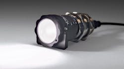
Demand for imaging in the SWIR range (between 1000 nm and 2000 nm), has increased in recent years. Sensors for these SWIR wavelengths prove critical in industries such as food inspection, giving the ability to see below the surface, for example, detecting bruises on apples earlier to stop an entire crop from going bad (Figure 1).
Similarly, the signature SWIR wavelength reflected by a substance (Figure 2) can detect and prevent poisonous food contaminants entering the supply chain. Doing so allows for a highly-cost-effective tool to identify even small amounts of a contaminant in even complex mixes. For example, a horsemeat contamination of beef can be identified using four wavelengths across the visible (515, 595, 650 nm) and SWIR (880 nm) wavelengths (bit.ly/VSD-HORSE).

Indeed, with hyperspectral imaging potentially set to play a key role in preventing future food contamination events it’s not a surprise that many governments—including the EU and US—have approved and are funding projects to further evaluate its potential – see the EU-supported Hypera project (bit.ly/VSD-EUFP), Kim Delwiche’s work for USDA’s Agricultural Research Service (bit.ly/VSD-USDA), and the Korean government-funded study to detect melamine in milk powder (bit.ly/VSD-MILK).
SWIR imaging also proves useful in security and astronomy, as well as in diverse sectors from silicon wafer and flat panel display inspection to art restoration and from drug discovery to autonomous vehicles, and has even been shown to visualize brain tumors and enable non-invasive detection (bit.ly/VSD-TUM).
Legacy SWIR sensor capabilities
Traditionally, image capture in the SWIR spectrum couldn’t be done using the same sensor technology as for visible light. Visible light applications (400 to 700 nm) typically use CMOS image sensors, a substrate that allowed the pixel pitch of visible light sensors to shrink quickly, giving ever greater resolutions. Additionally, CMOS gives a digital output. However, CMOS cannot capture light with wavelengths above 1100 nm.
To that end, SWIR imaging uses InGaAs technology. Legacy InGaAs technologies, however, suffered from low resolutions and the nature of the bump bonding process prevented further miniaturization (Figure 3). Additionally, this bonding process produced an analog output, and the structure of legacy InGaAs sensors prevented light in the visible spectrum reaching the photoelectric conversion layer.
Not only were resolutions kept low, it was also costly to create a hyperspectral camera capable of capturing both visible and SWIR light. Below, the article looks at how these three key limitations (resolution, sensitivity, analog output) can be addressed using a new process technology.
, while the right image shows the Cu-Cu connection.")
Resolution and miniaturization issues from the traditional bump connection between the InGaAs layer (where the photoelectric conversion takes place) and the readout circuit (Si layer) can be solved by adopting a Cu-Cu hybridization between a III-V InGaAs/InP of the photodiode array (PDA), and the Si layer.
This new approach was first outlined in December 2019 at the International Electron Device Meeting by a team of Sony researchers (bit.ly/VSD-SWIR) and allows the next generation of SWIR sensors to have higher pixel densities and enables the creation of smaller sensors and greater resolutions.
For context, SWIR chips using the legacy bump-bonding process have a pixel pitch of approximately 10 µm. Conversely, the first generation of SWIR sensors based on the new technology shrinks the pitch to 5 µm, enabling four times the number of pixels in the same space to create an SXGA (1296 x 1032) resolution SWIR sensor on a 1/2-type (8.2mm) footprint and a VGA (656 x 520) resolution sensor with a 1/4-type (4.1mm) footprint.
The ability to capture both SWIR and visible light on the same sensor reduces the cost for applications requiring hyperspectral images. Reducing the thickness of the InP layer, which for legacy sensors, was the key limiting factor in the amount of visible light that could penetrate it, makes this possible.
A thinner InP layer reduces the absorption of visible light and enables it to transmit to the InGaAs layer underneath, enabling imaging in a broad range of wavelengths from 0.4 μm to 1.7 μm (relative quantum efficiency >70% from 400 to 1650 nm). Additionally, this thinner InP layer also increases the relative quantum efficiency of SWIR wavelengths, with >90% of light from wavelengths between 900 to 1600 nm transmitting through the InP layer (Figure 4).
This improvement allows the sensor to capture both SWIR-visible light hyperspectral images to significantly reduce image camera-system processing loads, and overall system bill of materials vs multi-sensor solutions.
 wavelengths to penetrate to the InGaAs layer and be detected.")
Shifting to a Cu-Cu hybridization also allows the InGaAs sensor to output a digital signal without the use of a digital conversion circuit. This both simplifies design and gives SWIR cameras using this technology the same performance as current industrial CMOS image sensors.
Hyperspectral and SWIR technologies deliver significant benefits in food and agriculture for quality inspection and contamination detection but can be used across a wide range of industries – from art restoration to medicine to automotive.
By replacing bump connections with Cu-Cu bonding, it is possible to significantly improve on legacy InGaAs sensor limitations: quadrupling the pixel density, enabling SWIR and visible light capture on a single chip, and delivering a digital output.
Sony has launched its first two SWIR sensors based on this technology, with the sensors available from July: bit.ly/VSD-SONY.
Piotr Papaj is the European Communications Manager for Sony Europe (Weybridge, Surrey, UK,www.sony.com